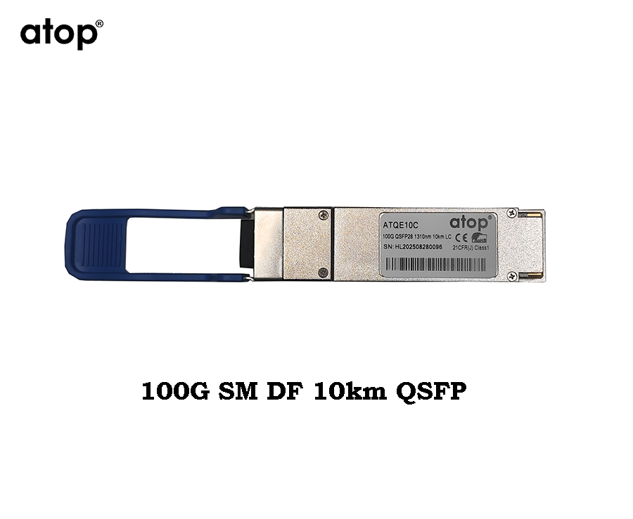
100G SM DF 10km QSFP

(0 reviews)
Estimate Shipping Time: 3 Days
Brand
atop
Warranty
1 Year Warranty

Inhouse product


Price
৳0.00 /pcs
Quantity
(110 available)
Total Price
Share

Features:

Hot pluggable QSFP28 MSA form factor

Compliant to IEEE 802.3ba 100GBASE-LR4

Up to 10km reach for G.652 SMF

Single +3.3V power supply

Operating case temperature: 0~70oC

Transmitter: cooled 4x25Gb/s LAN WDM EML TOSA (1295.56, 1300.05, 1304.58, 1309.14nm)

Receiver: 4x25Gb/s PIN ROSA

4x28G Electrical Serial Interface (CEI-28G-VSR)

Maximum power consumption 4.0W

Duplex LC receptacle

RoHS-6 compliant

Applications:

100GBASE-LR4 Ethernet Links

Infiniband QDR and DDR interconnects

Client-side 100G Telecom connections

1.        General Description:

This   product   is   a   100Gb/s transceiver   module   designed   for   optical communication   applications compliant to 100GBASE-LR4 of the IEEE P802.3ba standard. The module converts 4 input channels of 25Gb/s electrical data to 4 channels of LAN WDM optical signals and then multiplexes them into a single channel for 100Gb/s optical transmission.  Reversely on the receiver  side,  the  module  de-multiplexes a 100Gb/s optical input into 4 channels of LAN WDM optical signals and then converts them to 4 output channels of electrical data.

The central wavelengths of the 4 LAN WDM channels are 1295.56, 1300.05, 1304.58 and 1309.14nm as  members  of  the  LAN  WDM  wavelength  grid  defined  in  IEEE  802.3ba.  The  high  performance cooled   LAN   WDM   EA-DFB   transmitters   and   high   sensitivity   PIN   receivers   provide   superior performance for 100Gigabit Ethernet applications up to 10km links and compliant to optical interface with IEEE802.3ba Clause 88 100GBASE-LR4 requirements.

The product is designed with form factor, optical/electrical connection and digital diagnostic interface according  to  the QSFP+  Multi-Source  Agreement  (MSA).  It  has  been  designed  to  meet  the  harshest external operating conditions including temperature, humidity and EMI interference.

2. Functional Description:

The  transceiver  module  receives  4  channels  of  25Gb/s  electrical  data,  which are  processed  by  a  4-channel  Clock  and  Data  Recovery  (CDR)  IC  that  reshapes  and  reduces  the  jitter  of  each  electrical signal.  Subsequently,  each  of  4  EML  laser  driver  IC's  converts  one  of  the  4  channels  of  electrical signals  to  an  optical  signal  that  is  transmitted  from  one  of  the  4  cooled  EML  lasers  which  are packaged in the Transmitter Optical Sub-Assembly (TOSA). Each laser launches the optical signal in specific  wavelength  specified  in  IEEE802.3ba  100GBASE-LR4  requirements.  These  4-lane  optical signals will be optically  multiplexed into a single fiber by a 4-to-1 optical WDM MUX.  The optical output  power  of  each  channel  is  maintained  constant  by  an  automatic  power  control  (APC)  circuit. The transmitter output can be turned off by TX_DIS hardware signal and/or 2-wire serial interface.The receiver receives 4-lane LAN WDM optical signals. The optical signals are de-multiplexed by a

1-to-4 optical DEMUX and each of the resulting 4 channels of optical signals is fed into one of the 4 receivers that are packaged into the Receiver Optical Sub-Assembly (ROSA). Each receiver converts the optical signal to an electrical signal. The regenerated electrical signals are retimed and de-jittered and amplified by the RX portion of the 4-channel CDR.   The retimed 4-lane output electrical signals are  compliant  with  IEEE CAUI-4  interface  requirements.  In  addition,  each  received  optical  signal  is monitored by the DOM section. The monitored value is reported through the 2-wire serial interface. If one or more received optical signal is weaker than the threshold level, RX_LOS hardware alarm will be triggered.

A single +3.3V power supply is required to power up this product. Both power supply pins VccTx and Module Select (ModSelL) is an input pin. When held low by the host, this product responds to 2-wire serial  communication  commands.  The  ModSelL  allows  the  use  of  this  product  on  a  single  2-wire interface bus – individual ModSelL lines must be used.

Serial  Clock  (SCL)  and  Serial  Data  (SDA)  are  required  for  the  2-wire  serial  bus  communication interface and enable the host to access the QSFP28 memory map.

The ResetL pin enables a complete reset, returning the settings to their default state, when a low level on the ResetL pin is held for longer than the minimum pulse length. During the execution of a reset the host shall disregard all status bits until it indicates a completion of the reset interrupt. The product indicates  this  by  posting  an  IntL  (Interrupt)  signal  with  the  Data_Not_Ready  bit  negated  in  the memory map. Note that on power up (including hot insertion) the module should post this completion of reset interrupt without requiring a reset.

Low  Power  Mode (LPMode)  pin  is  used to  set  the  maximum power  consumption  for  the  product  in order to protect hosts that are not capable of cooling higher power modules, should such modules be accidentally inserted.

Module Present  (ModPrsL)  is  a  signal  local  to  the  host board  which,  in  the absence of  a  product,  is normally pulled up to the host Vcc. When the product is inserted into the connector, it completes the path to ground through a resistor on the host board and asserts the signal. ModPrsL then indicates its present by setting ModPrsL to a “Low” state.

Interrupt (IntL) is an output pin. “Low” indicates a possible operational fault or a status critical to the host system. The host identifies the source of the interrupt using the 2-wire serial interface. The IntL pin is an open collector output and must be pulled to the Host Vcc voltage on the Host board.

Pin Definition:


PIN

Logic

Symbol

Name/Description

Notes

1


GND

Ground

1

2

CML-I

Tx2n

Transmitter Inverted Data Input


3

CML-I

Tx2p

Transmitter Non-Inverted Data output


4


GND

Ground

1

5

CML-I

Tx4n

Transmitter Inverted Data Input


6

CML-I

Tx4p

Transmitter Non-Inverted Data output


7


GND

Ground

1

8

LVTLL-I

ModSelL

Module Select


9

LVTLL-I

ResetL

Module Reset


10


VccRx

+3.3V Power Supply Receiver

2

11

LVCMOS-I/O

SCL

2-Wire Serial Interface Clock


12

LVCMOS-I/O

SDA

2-Wire Serial Interface Data


13


GND

Ground


14

CML-O

Rx3p

Receiver Non-Inverted Data Output


15

CML-O

Rx3n

Receiver Inverted Data Output


16


GND

Ground

1

17

CML-O

Rx1p

Receiver Non-Inverted Data Output


18

CML-O

Rx1n

Receiver Inverted Data Output


19


GND

Ground

1

20


GND

Ground

1

21

CML-O

Rx2n

Receiver Inverted Data Output


22

CML-O

Rx2p

Receiver Non-Inverted Data Output


23


GND

Ground

1

24

CML-O

Rx4n

Receiver Inverted Data Output

1

25

CML-O

Rx4p

Receiver Non-Inverted Data Output


26


GND

Ground

1

27

LVTTL-O

ModPrsL

Module Present


28

LVTTL-O

IntL

Interrupt


29


VccTx

+3.3 V Power Supply transmitter

2

30


Vcc1

+3.3 V Power Supply

2

31

LVTTL-I

LPMode

Low Power Mode


32


GND

Ground

1

Reviews & Ratings

0.00 out of 5.0
(0 reviews)
There have been no reviews for this product yet.

Frequently Bought Products

All categories
Flash Sale
Todays Deal