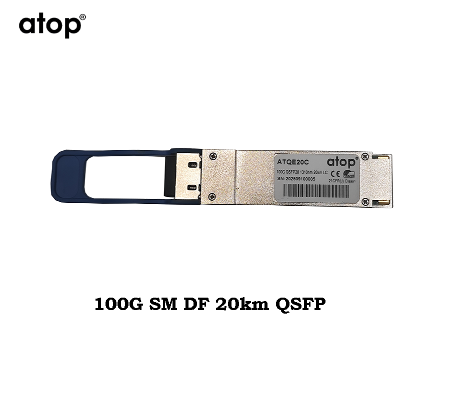
Inhouse product
² 4 lanes MUX/DEMUX design
² Integrated LAN WDM TOSA / ROSA for up to 20 km reach
over SMF
² Support 100GBASE-LR4 for line rate of
103.125Gbps and OTU4 for line
rate of 111.81Gbps
² Aggregate bandwidth
of > 100Gbps
² Duplex LC connectors
² Compliant with IEEE 802.3-2012 Clause 88 standard
IEEE 802.3bm CAUI-4 chip to module
electrical standard ITU-T G.959.1-2012-02 standard
² Single +3.3V
power supply operating
² Built-in digital
diagnostic functions
² Temperature range
0°C to 70°C
² RoHS Compliant Part
² Support FEC(Forward Error Correction)
² Local Area Network (LAN)
² Wide Area Network (WAN)
² Ethernet switches
and router applications
The QSFP28 100G LR4 is a
transceiver module designed for 20km optical communication applications. The design is compliant to 100GbASE-LR4 of the IEEE 802.3-2012 Clause
88 standard IEEE 802.3bm
CAUI-4 chip to module electrical standard ITU-T G.959.1-2012-02 standard . The
module converts 4 inputs channels (ch) of 25.78 Gbps to 27.95Gbps electrical
data to 4 lanes optical signals, and multiplexes them into a single channel for
100Gb/s optical transmission. Reversely, on the receiver side, the module
optically de-multiplexes a 100Gb/s input into 4 lanes signals, and converts
them to 4 lanes output electrical data.
The central wavelengths
of the 4 lanes are 1296 nm, 1300 nm, 1305 nm and 1309 nm . It contains a duplex
LC connector for the optical
interface and a 38-pin connector for the electrical interface. To minimize the
optical dispersion in the long-haul system, single-mode fiber (SMF) has to be
applied in this module.
The product is designed
with form factor, optical/electrical connection and digital diagnostic
interface according to the QSFP28 Multi-Source Agreement (MSA). It has been designed to meet the harshest external operating
conditions including temperature, humidity and EMI interference.
The
module operates from a single +3.3V power supply and LVCMOS/LVTTL global
control signals such as Module Present,
Reset, Interrupt and Low Power Mode are available with the modules. A 2-wire serial interface is
available to send and receive more complex control signals and to obtain
digital diagnostic information.
Individual channels can be addressed and unused channels can be shut
down for maximum design flexibility.
The QSFP28 100G LR is designed with form factor, optical/electrical connection and digital diagnostic interface according to the QSFP28 Multi-Source Agreement (MSA). It has been designed to meet the harshest external operating conditions including temperature, humidity and EMI interference. The module offers very high functionality and feature integration, accessible via a two-wire serial interface.
l Absolute Maximum Ratings:
|
Parameter |
Symbol |
Min. |
Typical |
Max. |
Unit |
|||
|
Storage Temperature |
TS |
-40 |
|
+85 |
°C |
|||
|
Supply Voltage |
VCCT, R |
-0.5 |
|
4 |
V |
|||
|
Relative Humidity |
RH |
0 |
|
85 |
% |
|||
|
Parameter |
Symbol |
Min. |
Typical |
Max. |
Unit |
|
Case operating Temperature |
TC |
0 |
|
+70 |
°C |
|
Supply Voltage |
VCCT,
R |
+3.13 |
3.3 |
+3.47 |
V |
|
Supply Current |
ICC |
|
1100 |
1500 |
mA |
|
Power Dissipation |
PD |
|
|
5 |
W |
l Electrical Characteristics (TOP = 0 to 70 °C, VCC = 3.13 to 3.47 Volts:
|
Parameter |
Symbol |
Min |
Typ |
Max |
Unit |
Note |
||
|
Data Rate per Channel |
|
- |
25.78125 |
|
Gbps |
|
||
|
|
|
27.9525 |
|
|
||||
|
Power Consumption |
|
- |
3.6 |
5 |
W |
|
||
|
Supply Current |
Icc |
|
1.1 |
1.5 |
A |
|
||
|
Control I/O Voltage-High |
VIH |
2.0 |
|
Vcc |
V |
|
||
|
Control I/O Voltage-Low |
VIL |
0 |
|
0.7 |
V |
|
||
|
Inter-Channel Skew |
TSK |
|
|
35 |
Ps |
|
||
|
RESETL Duration |
|
|
10 |
|
Us |
|
||
|
RESETL De-assert time |
|
|
|
100 |
ms |
|
||
|
Power On Time |
|
|
|
100 |
ms |
|
||
|
Transmitter |
||||||||
|
Single Ended Output Voltage Tolerance |
|
0.3 |
|
Vcc |
V |
1 |
||
|
Common mode Voltage Tolerance |
|
15 |
|
|
mV |
|
||
|
Transmit Input Diff
Voltage |
VI |
150 |
|
1200 |
mV |
|
||
|
Transmit Input Diff
Impedance |
ZIN |
85 |
100 |
115 |
|
|
||
|
Data Dependent Input
Jitter |
DDJ |
|
0.3 |
|
UI |
|
||
|
Receiver |
||||||||
|
Single Ended Output
Voltage Tolerance |
|
0.3 |
|
4 |
V |
|
||
|
Rx Output Diff
Voltage |
Vo |
370 |
600 |
950 |
mV |
|
||
|
Rx Output Rise and Fall Voltage |
Tr/Tf |
|
|
35 |
ps |
1 |
||
|
Total Jitter |
TJ |
|
0.3 |
|
UI |
|
||