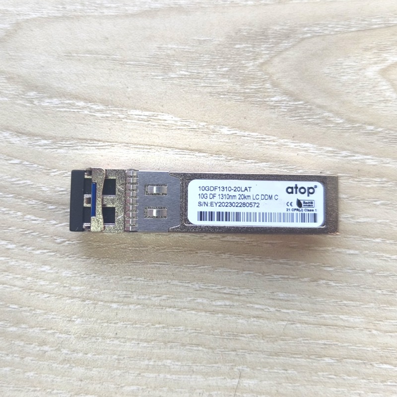
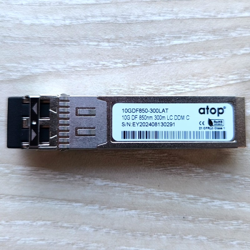
10Gbps SFP+ Optical Transceiver 20Km LC DDM
Features:
• Support 10GBASE-LR/10GBASE-LW/10G Fiber Channel application Compliant to SFP+ Electrical MSA SFF-8431
• Compliant to SFP+ Mechanical MSA SFF-8432 Multi rate of up to 11.3Gbps
• Transmission distance up to 20km (SMF)
• +3.3V single power supply Low power consumption
• Operating case temp: -5~+85°C RoHS 6/6 compliant
Absolute Maximum Ratings:
• Table 1- Absolute Maximum Ratings
Parameter Symbol Min. Typical Max. Unit Notes
Supply Voltage Vcc3 -0.5 - +3.6 V
Storage Temperature Ts -5 - +85 °C
Operating Humidity RH +5 - +95 %
Recommended Operating Conditions:
• Table 2- Recommended operating Conditions
Parameter Symbol Min Typical Max Unit Notes
Operating Case Temperature TC 0 - +70 °C
Power Supply Voltage Vcc 3.1 3.3 3.47 V
Power Supply Current Icc - - 300 mA
Power Dissipation Pd - - 1.0 W
Bit Rate BR - 10.312 - Gbp
Electrical Characteristics:
• Table 3- Electrical Characteristics
Parameter Symbol Min. Typ. Max. Units Notes
Transmitter
Differential Data Input Swing Vin,P-P 120 - 850 mVP
Input Differential Impedance ZIN 80 100 120 Ω
Tx_Fault Normal Operation VOL 0 - 0.8 V
Transmitter Fault VOH 2.0 - VCC V
Tx_Disable Normal Operation VIL 0 - 0.8 V
Laser Disable VIH 2.0 - VCC+0.3 V
Receiver
Differential Date Output Vout 100 - 800 mV
Output Differential Impedance ZD 80 100 120 Ω
Output Rise Time(20-80%) TR 24 - - ps
Output Fall Time (20-80%) TF 24 - - ps
Rx_LOS Normal Operation VOL 0 - 0.8 V
Lose Signal VoH 2.0 - VCC V
Transmitter Performance:
• Table 4- optical TX Characteristics
Parameter Symbol Unit Min Typ Max Notes
Optical transmitter Characteristics
Bit Rate BR Gbp 9.953 10.312 11.3
Center Wavelength Range λc nm 1290 1310 1330
Average Launch power Tx_off Poff dB - - -45
Launch Optical Power P0 dB -7.5 - 0 1
Extinction Ratio ER dB 3.8 - -
Jitter P-P JP ps - - 27
Note:
Jitter RMS JR ps - - 5
Optical Rise/Fall time Tr/tf ps - - 100
Eye Diagram Compliant With IEEE 802.3-2005
Optical receiver Characteristics
Bit Rate BR Gbp 9.953 10.312 11.3
Receiver Sensitivity RS dB - - -14.7 2
Overload Input Optical Power PIN dB 0 - - 2
Center Wavelength Range λc nm 1290 1310 1330
LOS LOSD dB - - -15.5
LOSA -24.5 - -
LOS Hysteresis dB 0.5 - -
1. Coupled into 9/125 SMF
2. Measured with PRBS 2 -1 test pattern @10.3125Gbps.BER=10E-12
Recommended Interface Circuit:
Recommended Host Board Power Supply Circuit:
Pin arrangement:
Table 5-Pin Function Definitions:
Pin Symbol Name/Description Note
1 VEET Module Transmitter Ground 1
2 TX_FAULT Module Transmitter Fault 2
3 TX_DISABLE Transmitter Disable; Turns off transmitter laser output 3
4 SDA 2-Wire Serial Interface Data Line (MOD-DEF2)
5 SCL 2-Wire Serial Interface Clock (MOD-DEF1)
6 MOD_ABS Module Absent, connected to VEET or VEER in the 2
7 RS0 module Rate Select 0, optionally controls SFP+ module
receiver as the following when HIGH input Bit Rate>4.25 Gbps
8 RX_LOS andwhenLOWinputBitRate≤4.25Gbps. ReceiverLoss of Signal Indication (in FC designated as RX_LOS, in SONET designated as LOS,
2
9 RS1 andin Ethernet designated as NOT Signal Detect) Rate Select 1, optionallycontrolsSFP+module transmitter as the
following when HIGH input Bit Rate>4.25 Gbps and when LOW input Bit Rate ≤4.25 Gbps.
10 VEER Module Receiver Ground 1
11 VEER Module Receiver Ground 1
12 RD- Receiver Inverted Data Output
13 RD+ Receiver Non-Inverted Data Output
14 VEER Module Receiver Ground 1
15 VCCR Module Receiver 3.3 V Supply
16 VCCT Module Transmitter 3.3 V Supply
17 VEET Module Transmitter Ground 1
18 TD+ Transmitter Non-Inverted Data Input
19 TD- Transmitter Inverted Data Input
20 VEET Module Transmitter Ground 1
Note:
1. The module ground pins are isolated from the module case.
2. The pins shall be pulled up with 4.7K-10Kohms to a voltage between 3.14V and 3.46V on host board.
3. The pin is pulled up to VCCT with a 4.7K-10KΩ resistor in the module.
Digital Diagnostic Memory Map:
Mechanical:
Order Information:
Part Number Product Description
10GDF1310-20LAT SFP+ 1310 nm 20km LC DDM
No Review Found.
Related Products
Sign up to newslatter
No Excuse Make Effort



Login To Comment