
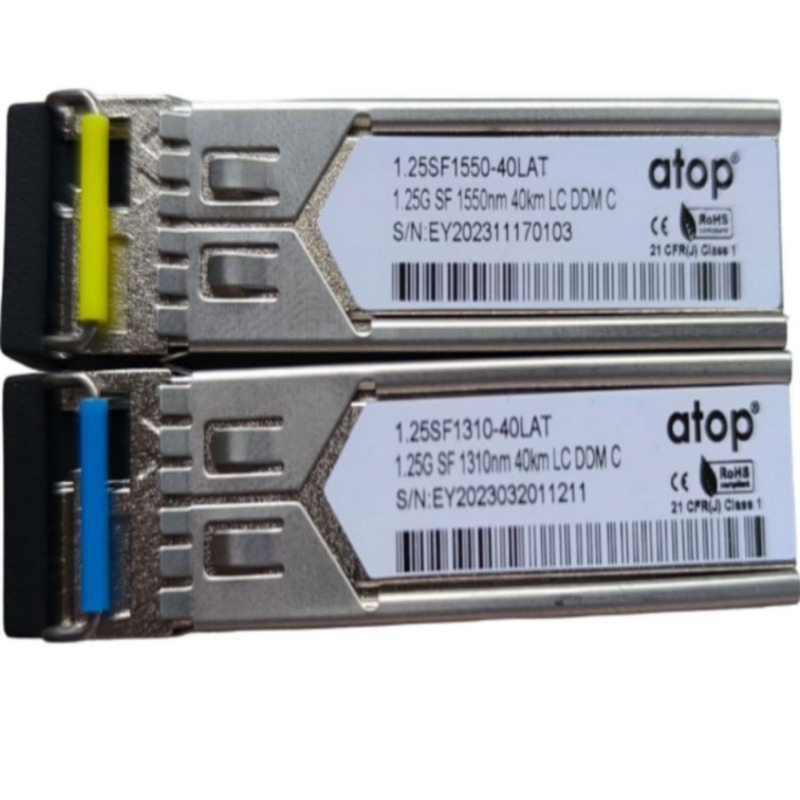
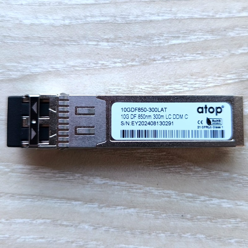
1.25Gbps SFP BIDI Optical Transceiver 20Km,40Km,80Km LC DDM
Feature:
Gi Obit Ethernet
Gi Obit Fiber Channel
SFP MSA package with Simplex LC connector
Compliant with IEEE 802.3ah,
Digital diagnostic monitor interface compatible with SFF-8472
transmission with 9/125 µm SMF
Single 3.3V Power Supply and LVTTL Logic
Very low EMI and excellent ESD protection
Operating Case Temperature: 0°C ~+70°C
RoHS compliant
Class 1 laser safety certified
Application:
Ethernet
Telecom
Fiber Channel
Absolute Maximum Ratings:
Parameter
Symbol
Mi
Ty
Max
Unit
not
l
n
p
e
Storage Temperature
Ts
-40
85
ºC
Storage Ambient Humidity
HA
5
95
%
Power Supply Voltage
VCC
-0.5
4
V
Signal Input Voltage
-0.3
Vcc+0. 3
V
Receiver Damage Threshold
5
dB m
Operation Environment:
Parameter
Symbol
Min
Ty p
Max
Unit
note
Case Operating Temperature
T case
0/40
70/85
Ambient Humidity
HA
5
70
%
Non-condensing
Power Supply Voltage
VCC
3.13
33
3.47
V
Power Supply Current
ICC
280
mA
Power Supply Noise Rejection
10 0
M V P-P
100Hz to1MHz
Data Rate
1.25
Gbps
TX Rate/RX Rate
Transmission Distance
0.55
120
KM
Coupled Fiber
Multi or Single mode fiber
Optical Characteristics:
(Ambient Operating Temperature 0˚ C to +70˚ C, Vcc =3.3 V)
Parameter
Symbol
Min
Type
Max
Unit
note
Average Output Power
Pout
-9.5
-3
dBm
0.55km 850nm
-9
-3
dBm
3km 1310nmFP
-9
-3
dBm
3km 1550nmFP
-9
-3
dBm
10km 1310nmFP
-9
-3
dBm
10km 1490nmDFB
-9
-3
dBm
10km 1550nmDFB
-2
+3
dBm
40km 1310nmDFB
-5
0
dBm
40km 1490nmDFB
-5
0
dBm
40km 1550nmDFB
-2
+3
dBm
80km 1490nmDFB
-2
+3
dBm
80km 1550nmDFB
Extinction Ratio
ER
9
dBm
Electrical Characteristics:
(Ambient Operating Temperature 0˚ C to +70˚ C, Vcc =3.3 V)
Parameter
Symbol
Min.
Typ.
Max.
unit
Transmitter Section
Input Differential Impendence
Zin
90
100
110
Ohm
Data Input Swing Differential
Vin
500
2400
mV
TX Disable
Disable
2.0
Vcc
V
Enable
0
0.8
V
TX Fault
Assert
2.0
Vcc
V
Deassert
0
0.8
V
Receiver Section
Output differential impendence
Zout
100
Ohm
Data Input Swing Differential
Vout
370
2000
mV
Rx LOS
Assert
2.0
Vcc
V
Deassert
0
0.8
V
Center Wavelength
λC
1270
1310
1360
nm
1310nm FP
1290
1310
1330
nm
1310nm DFB
1520
1550
1580
nm
1550nm DFB
Spectrum Width (RMS)
σ
4
nm
FP Laser (TX:1310nm)
Spectrum Bandwidth(-20dB)
σ
1
nm
1550nm DFB
1
nm
1490nm DFB
1
nm
1310nm DFB
Transmitter OFF Output Power
Poff
-45
dBm
Differential Line Input Impedance
Rin
90
10
0
110
0hm
Total Jitter (Peak-Peak)
tJ
41
PS
Note (1)
Output Eye Mask
Compliant with IEEE802.3z (class 1 laser safety)
Note (1)
Note: (1): Measure at 2^7-1 NRZ PRBS pattern Note (2): Transmitter eye mask definition
Specification of Receiver:
Parameter
Symbol
Min
Type
Max
Uni t
note
Input Optical Wavelength
λIN
1270
1310
1610
n m
Receiver Sensitivity
PIN
-22/-2 4
d Bm
15km~80kmNote (1)
-30
120km Note (1)
Input Saturation Power (Overload)
PSA T
- 3
d Bm
Los Of Signal Assert
PA
- 35
d Bm
PIN Receiver
Los Of Signal De-assert
PD
-25
d Bm
PIN Note (2)
LOS Hysteresis
PA-P D
0. 5
6
d B
Note (1): Measured with Light source 1550nm(1310nm), ER=10dB; BER =<10^-12 @PRBS=2^7-1NRZ Note (2): When LOS de-asserted, the RX data+/- output is High-level (fixed)
Electrical Characteristics:
(Ambient Operating Temperature 0C to +70C, Vcc =3.3 V)
Parameter
Symbol
Min.
Typ.
Max.
unit
Transmitter Section
Input Differential Impendence
Zin
90
100
110
Ohm
Data Input Swing Differential
Vin
500
2400
mV
TX
Disable
Disable
2.0
Vcc
V
Enable
0
0.8
V
TX Fault
Assert
2.0
Vcc
V
Deassert
0
0.8
V
Receiver Section
Output differential impendence
Zout
100
Ohm
Data Input Swing Differential
Vout
370
2000
mV
Rx_LOS
Assert
2.0
Vcc
V
Deassert
0
0.8
V
Epsom Information(A0):
Add
Field Size (Bytes)
Name of Fiel
HEX
Description
0
1
Identifier
03
SFP
1
1
Ext. Identifier
04
MOD4
2
1
Connector
07
LC
3-10
8
Transceiver
00 00 00 02 12 00 0D 0
Transmitter Code
11
1
Encoding
02
4B5B
12
1
BR, nominal
04 E2
1250M bps
13
1
Reserved
00
14
1
Length (9um)-km
14
20km
15
1
Length (9um)
64
16
1
Length (50um)
00
17
1
Length (62.5um)
00
18
1
Length (copper)
00
19
1
Reserved
00
20-35
16
Vendor name
57 49 4E 54 4F 50 20 20
36
1
Reserved
00
37-
39
3
Vendor OUI
00 00 00
40-55
16
Vendor PN
xx xx xx xx xx xx xx x x
ASC II
56-
59
4
Vendor rev
31 2E 30 20
V1.0
60-
61
2
Wavelength
05 1E/06 0E
1310nm/1550nm
62
1
Reserved
00
63
1
CC BASE
XX
Check sum of byte 0~62
64-
65
2
Options
00 1A
LOS, TX_DISABLE, TX_FAULT
66
1
BR, max
32
50%
67
1
BR, min
32
50%
68-
83
16
Vendor SN
00 00 00 00 00 00 00 00
Unspecified
84-
91
8
Vendor date code
XX XX XX 20
Year, Month, Day
92-
94
3
Reserved
00
95
1
CC-EXT
XX
Check sum of byte 64-94
Diagnostics:
Parameter
Range
Accuracy
Unit
Calibration
Temperature
C
-5 ~ 70
±3
ºC
Internal
I
-40 ~ 80
±3
Voltage
0 ~ VCC
0.1
V
Internal
Bias Current
0 ~ 120
±2
mA
Internal
Tx Power
-5 ~ 0
±1
dBm
Internal
Rx Power
<0
±1
dBm
Internal
Pin Description:
Pin
Symbol
Name/Description
Ref
1
VEET
Transmitter Ground (Common with Receiver Ground)
1
2
TFAUL T
Transmitter Fault.
2
3
TDIS
Transmitter Disable. Laser output disabled on high oropen.
4
MOD_ DEF(2)
Module Definition 2. Data line for Serial ID.
3
5
MOD_ DEF(1)
Module Definition 1. Clock line for Serial ID.
3
6
MOD_ DEF(0)
Module Definition 0. Grounded within the module
3
7
Rate Select
No connection required
4
8
LOS
Loss of Signal indication. Logic 0 indicates normal operation.
5
9
VEER
Receiver Ground (Common with Transmitter Ground)
1
10
VEER
Receiver Ground (Common with Transmitter Ground)
1
11
VEER
Receiver Ground (Common with Transmitter Ground)
1
12
RD-
Receiver Inverted DATA out. AC Coupled
13
RD+
Receiver Non-inverted DATA out. AC Coupled
14
VEER
Receiver Ground (Common with Transmitter Ground)
1
15
VCCR
Receiver Power Supply
16
VCCT
Transmitter Power Supply
17
VEET
Transmitter Ground (Common with Receiver Ground)
1
18
TD+
Transmitter Non-Inverted DATA in. AC Coupled.
19
TD-
Transmitter Inverted DATA in. AC Coupled.
20
VEET
Transmitter Ground (Common with Receiver Ground)
1
Notes:
Circuit ground is internally isolated from chassis ground.
Laser output disabled on T DIS >2.0V or open, enabled on T DIS <0.8V.
Should be pulled up with 4.7k - 10kohms on host board to a voltage between 2.0V and3.6V. MOD_DEF (0) pulls line low to indicate module is plugged in.
This is an optional input used to control the receiver bandwidth for compatibility with multiple data rates (most likely Fiber Channel 1x and 2x Rates). Ifimplemented, the input will be internally pulled down with > 30kΩ resistor. The input states are: Low (0 – 0.8V): Reduced Bandwidth (>0.8V,<2.0V):Undefined High(2.0– 3.465V):FullBandwidth Open: Reduced Bandwidth
LOS is open collector output. Should be pulled up with 4.7k - 10kohms on host board to a voltage between 2.0V and 3.6V. Logic 0 indicates normal operation; logic 1 indicates loss of signal.
Recommended Application Circuit: Outline drawing (mm):
Ordering information:
Part Number
Product Description
1.25SF1310-20LAT
SFP 1.25G Tx1310nm/Rx1550nm 20km LC DDM
1.25SF1550-20LAT
SFP 1.25G Tx1550nm/Rx1310nm 20km LC DDM
1.25SF1310-40LAT
SFP 1.25G Tx1310nm/Rx1550nm 40km LC DDM
1.25SF1550-40LAT
SFP 1.25G Tx1550nm/Rx1310nm 40km LC DDM
1.25SF1310-80LAT
SFP 1.25G Tx1490nm/Rx1550nm 80km LC DDM
1.25SF1550-80LAT
SFP 1.25G Tx1550nm/Rx1490nm 80km LC DDM
No Review Found.
Related Products
-0%
-0%
-0%

-0%
-4%
-0%
-0%
-0%
-0%
-3%
-0%
-2%
Sign up to newslatter
No Excuse Make Effort
Login To Comment